Search This Blog

Sunday 24 November 2013

Moments of my intimate contact with electricity: Touching Mosquito Racket Zapper net…

I knew it is a bad idea, that it is going to be painful… and yet the temptation was just too strong Smile
Plus – no harm for doing that right? After all, people accidentally does it once a while…

So with the power on – and closing in with index finger – I finally get closed enough – for a spark to “shoot” into my finger – and yap, it was painful – just like being poked by a needle! And it never cease to impress me what electronic can do, with couple of AA battery, this thing can boost it up to kV for zapping!
So this is where the boost converter comes in, with a boost converter, we can easily step up any voltage to the desired level, and it is pretty common in electronics (camera flash, spark plug….) And who says electronic is boring??

Monday 7 October 2013

About AC-DC Adaptor–Heavier is better

So i heard from a long time ago – when choosing a AC-DC adaptor – heavier is better. Really?

For a circuit guy – like myself – I think what the saying is really trying to tell you that AC-DC adaptor with transformer built in is better. For this I can’t agree more... from low level signal perspective.

For a +5V AC adaptor without transformer – each and every node inside the adaptor circuit is considered “LIVE” which means it is dangerous – the AC outlet voltage 230V for example is directly switched by silicon IC, and filtered to give a output of +5V. See schematic below:
image
(picture from some online forum.. sorry that can’t remember where I got it exactly, been with me for some time)

For a +5V AC adaptor with transformer – generally the transformer will scale down the line voltage to much managed able 12VAC or so, before passing it through bridge rectifier to and further drop down to +5V. So the secondary side of the transformer is not “LIVE” and much safer to mess around. Note that since the switching is done at much lower voltage level – the electrical noise will be much less. As shown below:
image

There are considerations on which is better – costing, how “clean” it is..., eventually it is up to the application and individuals to decide. For me, when I build something that requires mV or nA level of accuracy – those with transformer are definitely my choice of adaptor. Other than that, it does not bother me much.

I guess at the end of the day, knowing the fundamental of different AC adaptors allow an engineer to decide what is good enough for the application, and this especially important when dealing with low level analogue signals.

Friday 6 September 2013

Moments of my intimate contact with electricity:Telephone Line Voltage

I like wiring – since my childhood years – guess it is just the way i am.

One of my early experience as a teenager is to extend the telephone line – essentially i just strip the wires and twist the interconnect – with my bare hand. In the middle of doing that, muscle at my upper arm started twitching involuntary – it felt kind of funny – no pain but still… seeing part of your body behaving out of your control is kind of weird…

As it turns out, telephone line is typically at 40VDC, and when it rings it can go all the way up to 90VAC.. so i guess my twitching muscle act as the incoming call detector!! Smile

image

Having your body as part of current path is never a good idea, few mili ampere of current is enough to mess up your heart beat under the right condition – so give electricity some respect is what we should do..

Side notes:

from http://en.wikipedia.org/wiki/High_voltage

IEC voltage range AC DC defining risk
High voltage (supply system) > 1000 Vrms > 1500 V electrical arcing
Low voltage (supply system) 50–1000 Vrms 120–1500 V electrical shock
Extra-low voltage (supply system) < 50 Vrms < 120 V low risk

< 120VDC is considered as low risk.

What does equation y=mx+c got to do with specification?

Well, almost most of them. Take example, a voltmeter spec of +/-(10% of reading + 10% of range). The first term of % of reading is referred as gain error, and second term of % of range is referred as offset error.
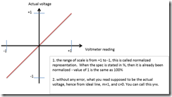
to understand this from graphical approach,
let’s start by drawing out a x-y axis – with x being voltmeter reading and y being actual value
then draw a line with y = x (implied m=1, c=0) from –1 to +1.
Let’s try to interpret this graph
image

now, to further discuss this, i think it is best to throw in some number – let’s consider the gain error of +/-10%. what it means is that the line will has a slope of 10% deviation from our ideal line (m=1, c=0).
if gain error is all that we have, then we have something like below:
image

next let’s consider the case where gain error is zero, and +/-10% of offset error (remember that we are taking about +/-10% of measurement range offset). for this we have
image
Now, for the real world instrument – gain error and offset error is real and cannot be ignored.
Factor in both gain and offset error, we have resulted in a series of possible lines that the real instrument behave.

image
From the look of it, it seem pretty bad – as the uncertainty is high for the voltmeter reading, in fact – up to 20% of measurement range. But, what you pay is what you get, gain and offset error of 10% is chosen for the sake of our discussion here. For real voltmeter with decent pricing, you can easily get 0.1% accuracy for both offset and gain. In certain case (depend of calibration, operating temperature, pricing…) you can even get better than 0.01%! Now, that is impressive.

Note:
In this example we used a voltmeter, but most measurement / sourcing instrument (source measure unit, power supply, oscilloscope, capacitance meter….) present their spec in similar form. So you can apply this method to have a sense of what the spec mean – with graphical approach.

Sometimes, the manufacturer will give un-normalized spec for offset, which is essentially the same thing. take our example here of +/-(10% reading + 10% of range) , if the range is 10V, the equivalent un-normalized spec will be +/-(10% reading + 1V)

Friday 2 August 2013

The Catches: Device Thermal Resistance

I been designing with power devices (BJT, Mosfet) for years – but I will always remember when I first started looking at their thermal resistance – by not reading through those fine prints,  I made gravely mistake of picking the wrong device for my prototype.

image
Take an example from the figure above – the device might be promoted to have less than 25degC per watt of junction-ambient thermal resistance (with fine print indicates test condition) – but without heatsink or large enough copper area, the thermal resistance easily go up to 40degC/Watt - as shown in the graph when copper area is less than 1 inches square.

Power dissipation specification at times shows best number - but only when mounted on large copper area - not practical for actual circuit – often heatsink is needed for low thermal resistance.

But it was the standard way for the industrial to compare using this method - too fresh and naive and some said silly to take it literally :)

Friday 5 July 2013

Opamp Level Shift & Scaling Circuit Analysis–Notes for Beginners

image_thumb
Follow up on previous post, a few points to note on algebra analysis - to state the obvious for those who already know, to clarify things for those with humble beginning like myself:
  • acknowledge consciously that the goal is to put variables into y = mx + c
  • you need to know at the end of derivation what is on the left hand side – in other words – you need to know what is going to be y, and x before you even derive it
  • always substitute repeating complex terms with a symbol – it keep you mind in the bigger picture – and save you from typo – or miss-spelled mistakes. You can always re-substitute the terms back at the end of derivation.
  • watch out for stuffs that can be derived from basics variable, and make use of them – for example, identify that Vdac is a function of Vref, and let Vdac = β*Vref, where 0<= β<=1.
  • always good idea to drop in some number to verify nothings goes wrong in the algebra derivation
  • take it easy – nobody is going to punish you if you get it wrong – have a bit of curiosity, have fun.

Saturday 15 June 2013

The Catches – Microcontroller Embedded I2C Module: My First Encounter with Errata-sheet

 
When I first started doing design works, there was this particular project that required me to communicate through I2C. It was my virgin experience using Microcontroller with embedded I2C engine– and it did not works well – errors occur intermittently – I spent 2 week checked and rechecked my codes, bus waveforms – start , stop, acknowledge conditions – every single thing that I could think of…

There was so much frustration, finally I told myself that enough is enough and there must be something else going wrong instead of my code – and Google long enough – I found out that there’s something called “Errata sheet”. And true enough – looking for the errata of that silicon revision on manufacturer’s website it showed that there was a bug in the silicon – and it proposed some work-around, plugged the workaround in and everything works accordingly Smile

Lesson learnt –
Before choosing a controller or similar devices – always read the errata (if it has one) for the stuffs that related to you, and newly released devices might be more happening that you would expect!


Monday 3 June 2013

The Catches: Safety Valve of Electrolytic Capacitor

Whether one believes in luck or not, for me there is no deniable that at times luck play a crucial part in life.

I remember my lucky escape from getting injured dealing with a boost converter with electrolytic capacitor. It was a brand new design – a boost that generate 100V. Something was not right – it could not go up to 100V – so I was having this board vised up ( to see what a “vise” is, go to http://en.wikipedia.org/wiki/Vise) is  to ease probing on each side – with those cap facing me (bad bad choice).

While I my face was inches away from the board – one of the cap exploded and shooting up hot boiling oily substance right pass me, hitting my cubicle wall about 1 meter way – it turns out that wrong part was installed – it was a 48V part.

It could at best cause some burnt on my not so handsome face – or at worst blinded me… come to think about that – I was simply lucky enough to escape un-injured and extremely thankful. To show you what i meant, i managed to find just a similar end result from wiki (http://en.wikipedia.org/wiki/Electrolytic_capacitor) as shown below:
image
Lesson learnt – those weak points being built on top of the capacitor can is the “safety valve” – it is designed to open up (“explode”) under overheat – overvoltage condition – never ever face the valve toward you or anybody else.


Sunday 26 May 2013

The Catches: Voltage follower that rings

In my first year doing circuit design – I was evaluating a circuit that contains a voltage follower op-amp – something that I didn’t quite happy with is the amount of overshoot on the step input. Digging through all the information – I found out that not op-amp are suitable for being a voltage follower. And in fact – for a voltage feedback op-amp to be used as voltage follower – it will state “unity gain stable” in the datasheet.
image
 
image
 
Lesson learnt –
There are certain amp that are not meant to be unity gain stable – mainly for fast response – read the datasheet before using them.


Opamp Level Shift & Scaling Circuit Analysis

image

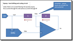
Generally DAC output will be from 0V to Vref, and to get bipolar output we typically use this circuit that convert [0:Vref] -> [-Vref: Vref], with Rf = Ri.

But what else can this circuit do if we are able to tweak Rf, Ri? Can it gives Vo > Vref?

There are few ways to get the transfer function of this circuit block, namely:

  1. circuit simulation - overkilled for such a simply circuit - don't you think so?
  2. algebra manipulation - going to be tough for those not doing it for a while
  3. graphical analysis base on circuit inspection - quick and intuitive - my personal favourite

in this example, I'm going to shows you alternative #2, and #3, have a nice read-up!


The algebra way:

Vo = Vdac + i * Rf
Vo = Vdac + [(Vdac-Vref)/Ri] * Rf
Vo = Vdac*(1+Rf/Ri) - Vref*(Rf/Ri)

but it is time consuming to write Rf/Ri, let's just replace it by α

Vo = Vdac*(1+α) - Vref*α

but Vdac is a function of Vref, let Vdac = β*Vref, where 0<= β<=1

Vo = β*Vref*(1+α) - Vref*α
Vo = Vref* [β + α*β - α]

where
α = Rf/Ri
β = dacData/dacFullResolution

it is always good idea to drop in some number to verify nothings goes wrong in the algebra derivation, let's do it now

let α = Rf/Ri = 1
Vo = Vref* [2β - 1]
β = 0: Vo = -Vref
β = 1: Vo = Vref
which is expected

Now that we have the final equation, we can inspect the equation as ratio of Rf/Ri changes:

Rf/Ri = 0:

  • Vo = Vref*β

Rf/Ri = infinity:

  • from Vo = Vref* [β + α*β - α]
  • when β = 0 (Vdac = 0): Vo = negative infinity
  • when β = 1 (Vdac = Vref): Vo = Vref

Conclusion:

from general equation of y = m*x + c, this circuit configuration allows us to configure maximum m = +1 @ c = 0, minimum m = negative infinity @ c = negative infinity, and max Vout = Vref.

For example, you are not getting more that Vo = Vref regardless of what Ri, Rf values you used.


The Graphical Way:


image

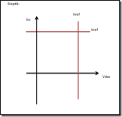
Step#1:

Figuring out what is input, what is output:

  1. draw out XY axis
  2. acknowledge that we control dac output directly, hence x-axis is label as Vdac
  3. Vo is the output of circuit block - we want to know what happen to Vo as Vdac changes - thus Vo as label for y-axis

Draw out the xy boundaries by circuit inspection:

  1. from circuit inspection - dac output can only varies between 0V to Vref, thus we draw at vertical line at x = Vref.
  2. from circuit inspection - when Vdac = Vref:
    • since inputs of op-amp is essentially the same potential - the inverting input is at Vref,
    • there is no voltage drop across Ri, both side of Ri at Vref, thus i=0A, and since there is no voltage drop across Rf, Vo=Vref
    • thus draw a horizontal lines at y = Vref

image

Step#2:

Acknowledge there is essentially one variable to play around - that is, the ratio of Rf/Ri :

  1. from circuit inspection - consider the case Rf/Ri = 0, it means Ri = open and i=0, and the amp act as voltage follower , Vo = Vdac, from y = m*x + c, this gives m =1, c =0, draw a line that cross point (x,y) = (Vref, Vref), (0,0), this is one of our boundary.
  2. from circuit inspection - consider the case Rf/Ri = infinity, when Vdac =Vref, Vo = Vref, when Vdac is slightly less than Vref, Vo = negative infinity, draw a vertical lines at x = Vref.
  3. region bounded by the 2 lines above is the possible circuit function for this circuit configuration. For example, you are not getting more that Vo = Vref regardless of what Ri, Rf values you used.

Wednesday 22 May 2013

The Catches: Boost Converter that don’t last

This happen about second year i started hands-on design – it was a 100V boost converter – most of the time the prototype works well – but every once a while – it stop working  after a large “blak” sound.

So tracing back on the switching waveforms – voltage, current I deduced that the inductance was not right – VL = L * (di/dt) relationship does not hold – drop in another piece – and it start working again.

Being curious as I am (luckily), I check the resistance of the inductor and compared to the new part (did not have LCR meter on hand). The resistance is much lower lower than the number stated in datasheet.

As the failure made me very un-comfortable – I went Google around – and it turns out that inductor does have voltage rating (although not mentioned in the datasheet of the one I was using), so the design was flawed in the first case – luckily it was found out earlier than later (it pays for being curious), else can’t even imagine what it would do in the field. Changing the part to high voltage part – and it work out solid!

For more details, refer to previous post: http://electroniccircuitdesignsharing.blogspot.com/2012/12/inductor-voltage-rating.html

Lesson –
Inductor does have voltage rating – due to the insulation coating of the windings, and the way wires being wound – and the inductor intended for high voltage operation will have working voltage stated in the datasheet – else don’t use it at high voltages.

Always look for the root-cause – it will save your ass


Saturday 11 May 2013

The Catches: My first encounter with Current Feedback Op-Amp

So to say, I was evaluating a circuit given in manufacturer’s reference circuit, being young and naïve (ignorant too), I just get the parts and put it in together – most of the time the circuit works – but when debugging one particular non-working circuit – something was not working accordingly.
So it was the time that I look at the datasheet of that amp – and found out that it was current feedback op-amp – not the assumed typical voltage amp – it turns out to be that current feedback op-amp are generally faster – and the behaviour differs as well.
for more details refer to wiki:
http://en.wikipedia.org/wiki/Current-feedback_operational_amplifier
Lesson Learnt:
Textbook op-amp circuit is generally voltage feedback op-amp – and there are much more in the market then what offered in text book.


Saturday 20 April 2013

About Debugging Guidelines

In debugging – sometimes I got carried away with my “instinct”, although mostly it get me to the right conclusion in a short time – it is definitely too much of “black magic” to the newbies.
So my humble advice to the beginners is to think about every circuit or IC as a functional block – define the boundary yourself or from a schematic – make sense of the circuit does. To state the obvious, in a typical circuit block:
  • will have a function name in the schematic - this contains important info regarding what the block supposed to do
  • will generally has input, output, supply and control signals
identify which is which will generally give you a sense of how to debug the block
clip_image002
Once you know that the input/output relationship does not hold (assuming that you understand what the block supposed to do), here are some of the steps that might helps
  1. Bias the circuit so that the block will have known state (or consider overwrite the input from a known source), use DMM to confirm all the DC pins, starting with supplies pins.
  2. Confirm the input output relationship – if it is not correct, break this block into smaller block and repeat the process (take a look at binary search debugging post: http://electroniccircuitdesignsharing.blogspot.com/2013/02/debugbinary-search.html).
  3. If the block is already an IC, check for part number, orientation, cold solder join, missing solder joints before “accusing” it as faulty part.
  4. remember that sometimes certain failure mode needs more than a DMM to be used (see http://electroniccircuitdesignsharing.blogspot.com/2012/06/why-oscilloscope-is-needed-for-circuit.html) , so if DMM cannot give you convergence, you should consider to use another instrument (depending on what this block supposed to do).
so good luck with your troubleshooting!


Saturday 6 April 2013

Thinking In Terms of Current– Photodiode Circuit Example

From the last post (http://electroniccircuitdesignsharing.blogspot.com/2013/03/thinking-in-terms-of-current.html) that talk about the importance of being able to think in term of current, now let’s look at particular example of circuit that basically manipulate current to get the desired result.

Shown below is a circuit that convert infrared light level into a voltage. Now, the photodiode convert infrared light density into current. This circuit is to provide a 0V bias across the diode (operate the diode in Photovoltaic mode) and convert the current into a low impedance voltage level for further operation.
image

In this circuit, the diode being used in Photovoltaic mode, and details about the diode operation can be found from http://en.wikipedia.org/wiki/Photodiode as shown below:
image

This is just one of many examples of the advantage being to think comfortably in term of current. Try to make sense of this circuit only thinking in voltage term will be a nightmare, since the inverting input of the op-amp supposed to be a “virtual ground”, and 0V across the diode does not make much sense.

Saturday 23 March 2013

Thinking In Terms of Current

Some years ago, there’s this movie called “Lost In Translation”, now, I have not watched it, but that reminded me of how I used to viewed or analyse circuit diagrams. During my early days – I cannot think or view the circuit in terms of current flow, as such everything being translated into voltage terms. Since DMM is handy for measuring circuit voltages – things looked good.
But as years goes by – when I got better in circuit understanding – I realize that by translating current into voltage (using resistance, impedance, equations), there are valuable circuit insights being lost in translation. For example – if you don’t think in terms of current flows – you cannot understand how decoupling works shown in previous posts:
http://electroniccircuitdesignsharing.blogspot.com/2012/07/3d-visualization-of-better-decoupling.html
http://electroniccircuitdesignsharing.blogspot.com/2012/07/3d-current-flow-for-inverting-op-amp.html
To show you what I meant, from my earlier post about load line: http://electroniccircuitdesignsharing.blogspot.com/2012/05/load-line-bjt-signal-gain-amplification.html
There is this BJT amplifier shown as below:
clip_image001
In this circuit – assuming that it is in linear region, collector current changes with base current directly, in fact Icollector = hfe * Ibase, where hfe is the current gain of BJT. Yes, Vout might be our parameter of interest, but it really is just a “byproduct” of this action: Vout = Vdd – (Ic * RC).
So for beginner – I would like to say when we view or analyse circuit – it is worth the effort to try to think in terms of current – it will open a whole new world.


Friday 1 March 2013

3D Perspective of Test Pen – And How It Works

I have always been fascinated by how a test pen works – since 12 years old, heck, i even tried to power up one with 2 AA batteries in series at age of 12!

As i found it tough to explain how it works, i been having this idea to draw it out in 3D, so finally i did it! Since this is related to high voltage stuffs, do read the disclaimer at the bottom of this page.

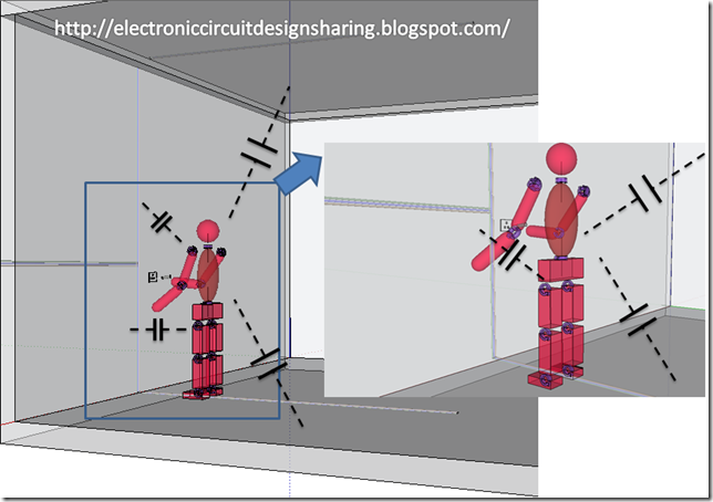
Look at the picture below, we have a test pen that light up when in contact with a "LIVE" or "HOT" wire, what's the magic behind it?
image

See picture below for the “BIG” picture. Through the body capacitance the AC current completed its path to Earth wire or Neutral wire, and light up the neon light inside the test pen.
image
In the picture, note that there are wires being routed inside the wall, floor, or ceiling, and in some cases the metallic piping under the floor will provide the return path for AC current as well.

See diagram below for the equivalent circuit:
image

Lots more info at link below:
http://en.wikipedia.org/wiki/Test_light

Saturday 16 February 2013

Debug–Binary Search

Sometimes, debugging of complicated circuits is an unavoidable task. To ease this process, some concept about binary search will proves to be helpful.
The idea about debugging using binary search as follow:
  • For a know series of circuit block that give un-expected result - always try to determine which half the the series that cause the problem
  • Repeat the iteration till faulty block found
For example:
In the diagram shown below, let x be the input, and output of each block be yn, where n is the block number, and block 15 coloured in red is the faulty block.
image
start: y16/x is not expected
  1. confirm y8/x is expected or not
  2. since y8/x is expected, we know the faulty block should be some where from block 9 to block 16, evaluate y12/y8
  3. since y12/y8 is working, faulty block should be some where from block 13 to block 16, evaluate block y14/y12
  4. y14/y12 is still working, faulty block should be some where from block 15 to block 16
thus regardless of where the faulty block is, the search terminate fast. In this example, if you were to use linear search method by evaluating from block #1 , block #2… , it will take you more time.

Sunday 3 February 2013

Debug – Inverting Op Amp

image
Let’s say you measured Vin = –1V, but Vout way off +1V, now what can be wrong? How do you debug it? Below are some suggestions for you to consider:
  • check the supply to see if the supplies are correct
  • visual inspect for
    • wrong polarity
    • wrong part (if manual assembly involved)
    • missing solder or “cold” solder
  • check if wrong resistors being loaded - power down – measure resistance of R1, R2 to see if any of R1, R2 is larger than 1KOhm – since this is in-circuit measurement – we don’t expect to see 1KOhm, but we definitely expect 1KOhm or less, since parallel resistance of any resistors is the minimum of those.
  • check if oscillation occurs - if everything looks good – get hold of a scope and confirmed there’s no oscillation on either pins mentioned above
  • check if op-amp already sourcing too much current - lift output pin, insert a small resistance resistor from pin to pad, measure the voltage drop to see if the amp is sourcing or sinking more that datasheet stated. It is possible that the next stage is demanding more current than expected.
So good luck with your troubleshooting Smile

Saturday 12 January 2013

Wolverine versus Real Life Capacitor

If you watch X-Men comics or movies, you know that Wolverine self heals, its his power. Believe it or not, some real life capacitor types also selfheal (if the damage is not too serious) – now is that amazing or what?
read more about this fantastic characteristic on links below:
http://en.wikipedia.org/wiki/Types_of_capacitor
http://www.ehow.com/list_7686462_self-healing-properties-capacitors.html
Marvelwolverine.jpg
picture from http://en.wikipedia.org/wiki/Wolverine_(comics)