Have you ever wonder that when you read through datasheet for inductors, you rarely see the voltage rating?
Shown in picture below are some common inductors seen.
The fact is, inductor does have voltage rating, the winding wire have a fix thickness of insulation coating, if high enough voltage is applied across the inductor, although momentary and the current is within the specification limit, the insulation will breakdown and short to adjacent wire. From personal experience, normally inductor voltage is about 60V, unless specifically stated in datasheet. Maximum voltage allowed is usually depends on insulation thickness of wire used, and whether the windings overlap.
If you does wonder whether your inductor has insulation breakdown, the easiest way is to measure DC resistance, depending of actual short, the resistance will be a lot or somewhat lower than a good one. Alternately, if you have a LCR meter, you can use it to measure the inductance instead, in this case, expect faulty inductor to have lower inductance (less winding over the magnetic core).
Search This Blog
Saturday, 29 December 2012
Saturday, 22 December 2012
Real Life Inductor : When Does An Inductor Stop Behaving Like One
- When current is too high – because of magnetic saturation
- When signal of interest is of too high frequency – higher or near inductor self resonant frequency. There are parasitic capacitance across inductor winding so in a way, we have parallel LC circuit, at high enough frequency, the impedance of C will gets low enough to shunt out the impedance of inductor.
Friday, 7 December 2012
What does SCR protection circuit has in common with reactive armour tanker?
SCR is a circuit component that conduct when it is been triggered. typical circuit is as shown below:
When there's overvoltage across Rload, zener Z1 will conduct and trigger SCR X1 into conduction - this cause huge current that blow the fuse.
Without this protection, the current level during over voltage might be too little for fuse to burn open
Now compare this protection mechanism with explosive (reactive) armoured tank shown below (picture from http://en.wikipedia.org/wiki/Reactive_armour).
Those “bricks” are actually explosive material. When the tank being hit by bazooka, the plate will explode, thus dispersing the piercing force of the bazooka, and thus preventing injury for personnel in side.
Both SCR protection (with fuse) and reactive armour protection work in similar way – namely by conducting large amount of current to burn fuse versus exploding of “brick” to disperse piercing force of bazooka– to protect the cargo, by preventing the destructive force from 'hurting’ the cargo.
Friday, 23 November 2012
Source and Load Matching: Cyclist Perspective
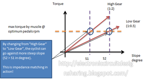
If you ever ride a bicycle – you know how amazing that a bicycle with gear allow you to “match” your muscle (energy source) to any landscape (load). Essentially the gear match the source to load just like the way transformer match an AC source to its load.
Let’s look at a simplified diagram of the torque that your leg muscle generate versus the landscape – slope degree.
Assuming that at gear ratio of 1:1, for every turn of pedals the wheel will turn by one cycle, then:
Low Gear (1:0.5) means for every turns you make on the pedals, the wheel only make half a turn, since your leg muscle power is constant, your loss on speed is made up with your increase of forward force.
High Gear (1:2) means for every turns you make on the pedals, the wheel only make 2 turns, since your leg muscle power is constant your gain on speed is made up with your reduction of forward force.
Now compare this to the impedance matching in audio amplifier:
Picture from Wikipedia - transformer to perform impedance matching
Saturday, 10 November 2012
Source and Load Matching: DC perspective
Have you ever wonder why people talk about source and load matching? I did, and one thing that I asked my self is whether I have something in DC domain that can help me to visualized it. Well see below for my way of understanding source and load matching.
Supposed that we have a circuit as shown below:
From there we can create a table of maximum possible power that Rl can pull out of the source Vs:
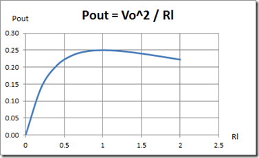
From the table we can plot out the load power as Rl changes – as you can see, max Pout occurs when Rl “match” Rs, which is 1 Ohm in this example
Supposed that we have a circuit as shown below:
Vs | Rs | Rl | Vo = VS * (Rl/(Rs+Rl)) | Pout = (Vo^2)/Rl |
1 | 1 | 0 | 0.00 | - |
1 | 1 | 0.2 | 0.17 | 0.14 |
1 | 1 | 0.4 | 0.29 | 0.20 |
1 | 1 | 0.6 | 0.38 | 0.23 |
1 | 1 | 0.8 | 0.44 | 0.25 |
1 | 1 | 1 | 0.50 | 0.25 |
1 | 1 | 1.2 | 0.55 | 0.25 |
1 | 1 | 1.4 | 0.58 | 0.24 |
1 | 1 | 1.6 | 0.62 | 0.24 |
1 | 1 | 1.8 | 0.64 | 0.23 |
1 | 1 | 2 | 0.67 | 0.22 |
From the table we can plot out the load power as Rl changes – as you can see, max Pout occurs when Rl “match” Rs, which is 1 Ohm in this example
Friday, 19 October 2012
Be thankful of AC transmission line
Recently I came across some pictures during Edison’s day, where the power line was in DC. Since there are lots of power loss (see Why Transfer Power At High Voltage), lots of cabling were required for power transmission. And the end result? Below is the picture that I managed to Google. At that time, in some part of the city people literally cannot see the sky!
Picture from wiki : http://en.wikipedia.org/wiki/Electric_power_transmission
Sunday, 14 October 2012
Impedance matching–What does a mountain bicycle has in common with a transformer
As a cyclist and a transformer user, can’t help to notice the similarity of the two. So below is the picture of a mountain-bicycle and transformer taken from my favourite source Wikipedia.
To compare them, look at the table of comparison below:
A Bicycle | A Transformer |
number of “teeth” of sprocket | number of winding |
front sprocket | primary winding |
rear sprocket | secondary winding |
gear chain | transformer core |
now, isn’t this amazing?
To understand sprocket, visit http://en.wikipedia.org/wiki/Sprocket
Pictures from :
http://en.wikipedia.org/wiki/Bicycle
http://en.wikipedia.org/wiki/Transformer
To understand sprocket, visit http://en.wikipedia.org/wiki/Sprocket
Pictures from :
http://en.wikipedia.org/wiki/Bicycle
http://en.wikipedia.org/wiki/Transformer
Friday, 5 October 2012
Getting to know simulation - Part11 - Monte Carlo
To best
illustrate the usefulness of the monte-carlo
simulation, let’s use a voltage divider as example.
Run Transient simulation and get:
So this is
a perfect voltage divider. But we all knows that resistor has tolerance, let’s
say each of R1, R2 has 1% tolerance. We should factor this in by running Monte Carlo simulation and see what are we dealing with.
Enter 1% as
the resistor tolerance.
Tick “Enable
multi-step” to enable Monte-Carlo analysis
Set number
of runs to 100
Re-run the
transient simulation to see gain statistic of divider made of 2 pieces of 1% resistor.
With resistor tolerance of 1%, the voltage divider will give an error of ~-0.9% to ~+1%.
Use of Monte-Carlo simulation will ease such analysis. If your application cannot tolerate such variance, then resistors with better tolerance are needed.
Friday, 28 September 2012
Getting to know simulation - Part10 - Multi-Step
So continue from previous session, inserting C2 1nF to kill oscillation gives you the stability but make your buffer damn slow. You can try out few value to see the optimum C2 value for highest speed and still gives you the best stability, instead of manually change the values and re-run Transient Simulation, there is something called “Multi-Step” analysis that let you sweep any parameter and plot the result.
1. Open up analysis and tick “Enable multi-step”
2. Click “Define…” button and key in the info as below:
Saturday, 22 September 2012
Getting to know simulation - Part9 - Fixing oscillation
1.
There are plenty of ways to resolve this, one way is to add a capacitor in parallel with feedback
resistor R2. Let’s do this in the schematic and re-do the AC simulation. At
this point of time, the value of C2 is arbitrary chosen to be 1nF, we will talk
more about this in next session – any way the latest schematic becomes:
2.
Re-do the simulation for AC with simulation
frequency up to 10MHz to see the new closure-
you can see now that the rate of closure becomes 20dB / decade
– indicating stability has achieved, let’s modify the schematic to re-do the
transient
3.
To look at the end result of the fix in time
domain, insert 1nF for the transient simulation file:
4.
Re-run of transient simulation shows that so we have
solved the problem of oscillation – but the problem is that the output of the
buffer takes 4ms to settle to the right value – too slow for our liking – this
we will try to solve in next session.
Friday, 14 September 2012
Getting to know simulation - Part8 - Arranging bode plot for AC analysis
1.
The best way to do AC stability analysis to plot Aforw vs
1/beta, plot of 1/beta essentially is the inversion of the beta gain – which is
input/output instead of output/input – so let’s reverse the bode plot and rename the block as shown
2.
So now you can see that the 40dB per decade closure of
Aforw and 1/beta is the cause for oscillation
Friday, 7 September 2012
Getting to know simulation - Part7 - Bode Plot from a buffer circuit (that oscillate)
Continue
from last post, to solve the problem, we need to acknowledge that the buffer
circuit is in fact a feedback loop
To identify
which components belong to with block – refer to the blog
Let’s modify the schematic to perform bode plot analysis
1.
Ground non-inverting input – since op-amp input
is already high impedance – any voltage source with series resistance is pretty
much behaving just like a pure voltage source – for DC voltage source, it is
always a AC ground.
2.
Place large inductor, infinite AC coupling
capacitor and AC source, configure the AC source as below:
3.
Choose AC analysis:
4.
Your schematic should becomes:
5.
After simulation, you get
6.
But, how to interpret the plot?
Sunday, 2 September 2012
Getting to know simulation - Part6 - Practical circuit consideration
Continue from last simulation done in Part5, the simulation result shows that the
circuit is too ideal – in practical PCB, there will be about 10pF of
capacitance from op amp input pin to GND, let’s insert this capacitance as
below:
Re-run the
transient and get:
In this
case, we caught the potential issue - oscillation – as to solve it, let’s do it in the next
posts.
Saturday, 25 August 2012
Getting to know simulation - Part5 - Transient Simulation
So far so
good for DC, but we still need to know the characteristic for fast changing sensor output – what’s the
waveform going to be. Let us replace Vsensor from DC
1V to Step 1V by double click on the source and configure the output to be 1V Step
voltage with 2ms delay:
To ease
subsequent examples about simulation, change some of the op amp settings by
double click on it, change as below:
To plot the
waveform, insert a probe at the output of buffer (short cut “B”)
Then choose
Transient analysis:
And you
would get nice waveform as shown below:
So far so good - but is it too good to be true?
Getting to know simulation - Part4 - insert basic buffer amplifier
To continue
from previous post, let’s modify the circuit above as below
1.
Insert
a parameterised opamp from menu Place –> Analog Functions -> Parameterised Opamp
2.
Insert
a +/-15V DC supplies from menu Place –> Voltage Sources -> Power Supply
3.
Insert
off-page connectors from menu Place -> Connection -> Terminal
4.
Wire
up the opamp as x2 buffer amp using 1Meg Ohm resistors (so that 1V full scale
sensor output will translate to 2V full scale ADC input). Route the circuit
accordingly, re-run DCOP simulation and you get:
Now with
the buffer – we get pretty good DC result – 1V sensor translated into ~2V adc input. For now, don’t concern yourself with the ~20mV
error (2V – 1.97997V), we will cover this some other time.
Saturday, 18 August 2012
Getting to know simulation - Part3 - using DCOP
Let’s look
at the reason we need to design the buffer. If we direct connect the sensor to adc input –
We will
have 1V * 1k/(100k + 1k) ~= 10mV only, clearly this is
not acceptable. Note that in Mindi, instead of using R1, R2 ... you can right click on component and change its name, in this case Radc is the name chosen to represent the ADC.
To simulate
– all spice required “Ground” symbol for reference, so let’s insert one as
below, double click on V1 and rename it to Vsensor, and change name of R1 to Rout.
We want to
know the voltage at ADC input, so place voltage marker on the interconnect node
for Rout, Radc to see the voltage
Schematic after
placing marker:
Then choose
simulation mode to be DCOP
And click “Run”
Now you see
the need for buffer circuit. DCOP is the first thing that I recommend for any
simulation, since it let you see the DC biasing in the schematic itself – especially when the
circuit is much more complicated than this. You can place as many markers as
required.
Getting to know simulation - Part2 - Modeling
Let’s get
started by modeling the blocks in schematic – knowing how to model is critical – else it will be GIGO (Garbage-In-Garbage-Out).
1.
Modeling
of the sensor to ease design process – if you look at sensors such as
microphone, transducer, you would find that most of them if not all do not have
“Low output impedance”, which means, you cannot use a voltage source to model
it. So let’s model our sensor as below, the values of R1, R2 is not important,
which will become clear at this end of the series: in this case,
output of the sensor is 1V.
2.
As
for the ADC, to ease design process
let’s use a 1kOhm resistor to represent it – it is the load of the buffer
circuit, at the end of the series, you will know why this is good enough
Getting to know simulation - Part1 – Introduction
Getting to know simulation - Part1 –
Introduction
In circuit design - simulation tools will ease your
life a lot - if you know what you are doing. As such I am writing a series of
posts that I hope will best help you to understand what you can do with
simulation - by using a buffer amplifier design example. The goal is to
introduce basic features such as
- DCOP
- TRAN
- AC
- Multi-Step
- Monte-Carlo
Let’s take an example as below:
1.
Supposed that we need to design something
that interface a sensor to ADC, so we have
a.
sensor
b.
The ADC
c.
And something in between – a voltage buffer – and this is what we need to design
2.
To supplement the design example, let’s
put some more details
a.
Sensor bandwidth is at least 10kHz
b.
Sensor can swing from 0V to 1V
c.
ADC full range voltage is 0V to 2V.
Since I am a user of Mindi from Microchip, I will use Mindi as examples,
but essentially all simulation tools have the basic set of features. If you
want, you can install Mindi mentioned from my earlier blog (In this case, you can quickly test out the
example): http://electroniccircuitdesignsharing.blogspot.com/2012/03/tools-for-circuit-design.html.
Alternately, you can down load SIMetrix from http://www.simetrix.co.uk/site/demo.html, which is essentially the same thing as Mindi (just the name different as far as I am concerned, same GUI, same file type....)
My advice
is to play around with your simulation tools, knowing the capability of what it
can do will make your life a lot more fun :). So wait for Part 2 to get
started.
Subscribe to:
Posts (Atom)